Samsung expands glass carrier capacity to more than double HBM4 output
Samsung will raise outsourced glass carrier cleaning volume to 50,000 sheets a month next year, a step industry sources say points to at least a doubling of HBM4 and HBM4E chip output.
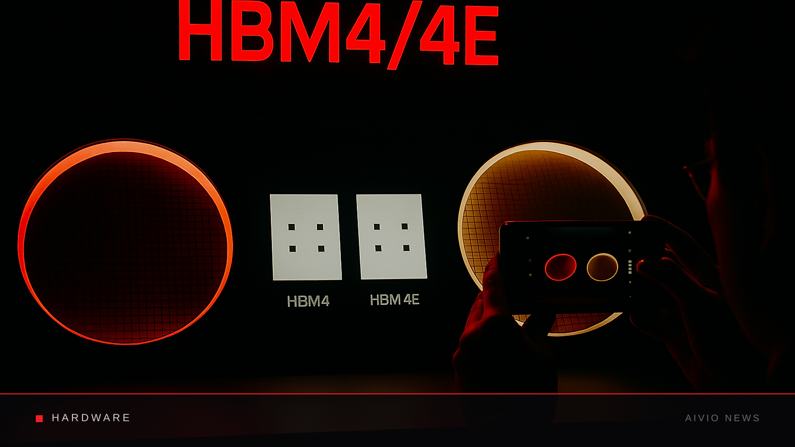
Samsung Electronics is expected to more than double production of its HBM4 family of memory chips next year, according to semiconductor industry sources cited by Seoul Economic Daily on September 20. HBM, or high-bandwidth memory, is a type of chip that stacks multiple DRAM layers to move data faster, and it is a core component in the processors used for AI computing.
The increase is tied to glass carriers, a material used while HBM wafers are ground thin and drilled to allow dense stacking. A glass carrier is temporarily attached to the underside of a wafer to keep it from bending or cracking during that process. According to the sources, Samsung will raise its outsourced cleaning volume for glass carriers, which are reused after cleaning, to 50,000 sheets a month next year from 20,000 sheets a month this year. That volume had stood at just 10,000 sheets a month as recently as last year before doubling this year.
Industry analysts say that even factoring in reuse of carriers and differences in consumption tied to process methods and yield, a 2.5-fold rise in glass carrier volume makes it highly likely that Samsung’s output of HBM4 and seventh-generation HBM4E will grow at least twofold from this year. The chips at the center of the buildup are built on 12-layer and higher stacks, which require tighter control over wafer thinning and warping as more dies are packed into a limited thickness.
Mass production already underway
Samsung began mass-production shipments of HBM4 in February, using 10-nanometer-class sixth-generation DRAM paired with a base die built on a 4-nanometer process. In May, the company also began providing 12-layer HBM4E samples to customers, including Nvidia, according to the report.
The broader production picture points in the same direction. Industry sources expect Samsung’s total HBM output, measured by average monthly wafer input, to grow nearly 40% next year, to about 250,000 wafers from roughly 180,000 wafers this year. Within that, the HBM4 family’s share of shipments is projected to rise from about 40% this year to about 80% next year as HBM4E mass production ramps up. “As Samsung expands HBM production, it appears to be placing HBM4, a high-value product, at the center,” an industry official told the outlet.
None of the figures in the report are confirmed by Samsung itself, and the sourcing rests on unnamed semiconductor industry contacts rather than company disclosure. What to watch next is whether Samsung confirms a formal capacity target in an earnings call or investor filing, how HBM4E qualification with customers like Nvidia progresses toward volume orders, and whether the 250,000-wafer figure holds up as next year’s production plans firm up.
Sources
AI-generated · AIVIO News Desk